
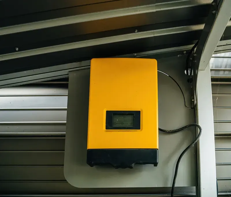
How Many Layers of PCB Are Used in Solar Inverters
The answer to this question is quite variable because the layer number highly depends on different factors such as power level, topologies, control schemes, and reliability requirements.
Usually, one-layer or even two-layer PCB design is never used for building the solar inverter's board. In the vast majority of cases, solar inverters make use of multilayer PCBs because of their higher power density, immunity to electromagnetic interference, and ability to implement complex control circuits.
Why Layer Number Matters in Solar Inverter Design
The choice of PCB layers is crucial for performance, safety, and durability in a number of ways.
Electrical performance and signal integrity
The solar inverter uses high voltage and sensitive control circuitry. To ensure reliable work of control circuits despite high power switching, engineers make use of multilayer PCB design where:
- There are several power planes
- Separate ground planes exist
- Signal routing is possible
Thermal management and reliability
Heat is a constant challenge in solar inverters. More PCB layers enable:
- Better heat distribution
- Dedicated copper planes for thermal spreading
- Reduced hot spots
The study titled A Review of Power Electronics for Grid Integration of Solar Photovoltaic Systems, published by IEEE, shows that increasing power density and switching frequency in solar inverters significantly raises design complexity, which directly influences PCB structure and layering decisions
Typical PCB Layer Counts in Solar Inverters
While there is no universal benchmark, practice in the industry reveals distinct trends depending on the types of inverters and their complexity.
Residential inverters (1-3 kW)
In these cases, the following board stack-ups are generally observed:
- 2 to 4 layers for control circuit boards
- 2 layers for auxiliary circuits
The main goal at this point is to achieve cost-effective design. Still, even for low-power applications, multi-layer PCB technology is widely used due to noise management issues.
Mid-level inverters (3-20 kW)
Multi-layer PCB design starts at this level:
- 4 to 6 layers for control and drive circuitry
- Power and control boards are separated from each other
Cost optimization meets performance requirements at this stage, and noise suppression becomes essential.
Commercial and industrial level inverters
For powerful industrial systems, we observe:
- Control PCBs made up of 6 to 12 or more layers
- Gate drivers can use high-density layer count PCBs
Industrial power converters operate in extreme conditions of high voltage and current, along with continuous operation.
Key Factors That Determine PCB Layer Count
Instead of demanding the layer count, it is better to find out why there are many layers.
Power rating and voltage level
The higher the power rating:
- The thicker the current traces will be
- The stronger the electromagnetic interference will be
- The higher the insulation demands will be
It will all force engineers to create multilayer PCBs.
Switching frequency
Solar inverters that operate on the principle of high-frequency switching become popular:
- The design constraints become tighter
- Noise coupling issues become a problem
Multilayer boards help solve both of these problems.
Control functionality
New intelligent inverters have many additional functions such as:
- Digital signal processors (DSPs)
- Communication channels
- Monitoring sensors
These functions usually need multilayer circuit boards.
Regulatory and safety aspects
There are stringent requirements for inverters connected to the grid. Multilayer boards can provide:
- Creepage and clearance handling
- EMI compliance
- Robustness
Power Board vs Control Board: Different Layer Needs
It is vital to recognize that there are several types of PCBs used in solar inverters.
Power Boards
They deal with high currents and voltages and usually have:
- Less layers (2-4)
- Heavy copper
- Wide traces for insulation purposes
Current management is a key objective here; not rout density.
Control and signal boards
They are intricate and have:
- 4-12 layers
- Specific ground and power planes
- Fine-pitch routing
Here lies the bulk of multi-layer intricacy.
Why Solar Inverters Rarely Use Single or Double Layer PCBs
A reduction in layers appears to be more economical at first sight, but not in solar inverter design.
Problems Related to Noise and EMI
With no adequate layer isolation
- Switching noise will interfere with control circuits
- The system will lose stability
Routing restrictions
Today’s advanced parts need extensive connections. A two-layer board cannot accommodate
- High-pin-count chips
- Feedback circuits
Reliability problems
A bad design results in
- Thermal strain
- Misleading signals
- Potential system malfunction
In most real-world designs, the cost savings of fewer layers are quickly offset by performance and reliability problems.


Emerging Trends in PCB Design for Solar Inverters
The industry is changing, and so is PCB design.
High integration and small form factors
With the shrinking size and increasing power density of inverters:
- More layers are being used
- Boards are getting smaller
Wide bandgap semiconductors
With technologies such as SiC and GaN comes:
- Faster switching frequencies
- Better efficiency
But they require more careful PCB layout designs, sometimes necessitating extra layers.
Digitalization and smart grid capabilities
Contemporary inverters have incorporated:
- Internet-of-things capability
- Real-time sensing
- Sophisticated control schemes
These add to the intricacy of PCB design.
How Many Layers Should You Expect?
If one figure is needed, then it may safely be said that:
- 2 -4 layers for simple, low-power converters
- 4 -6 layers for most homes and standard inverters
- 6 -12 or more layers for performance or heavy-duty inverters
But this approach would mislead if taken literally. The layer count is always determined by the specific needs of the design.
Choosing the Right PCB Complexity
The number of layers of a printed circuit board (PCB) used for a solar inverter is never an unnecessary thing. Instead, each extra layer provides a particular solution related to noise handling, heat dissipation, or signal routing.
If you are considering or designing a solar inverter, think about:
- Power capacity and switching performance
- Control scheme difficulty
- Regulatory compliance
After that, choose the corresponding PCB structure. Generally, starting with a few layers of PCB at the beginning of the development process can result in a more reliable device later.
About the Author